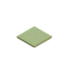
The low-cost AM62x Sitara™ MPU family of application processors are built for Linux® application development. With scalable Arm® Cortex®-A53 performance and embedded features, such as: dual-display support and 3D graphics acceleration, along with an extensive set of peripherals that make the AM62x device well-suited for a broad range of industrial and automotive applications while offering intelligent features and optimized power architecture as well.
Some of these applications include:
- Industrial HMI
- EV charging stations
- Touchless building access
- Driver monitoring systems
AM62x Sitara™ processors are industrial-grade in the 13 x 13 mm package (ALW) and can meet the AEC-Q100 automotive standard in the 17.2 x 17.2 mm package (AMC). Industrial and Automotive functional safety requirements can be addressed using the integrated Cortex-M4F cores and dedicated peripherals, which can all be isolated from the rest of the AM62x processor.
The 3-port Gigabit Ethernet switch has one internal port and two external ports with Time-Sensitive Networking (TSN) support. An additional PRU module on the device enables real-time I/O capability for customer’s own use cases. In addition, the extensive set of peripherals included in AM62x enables system-level connectivity, such as: USB, MMC/SD, Camera interface, OSPI, CAN-FD and GPMC for parallel host interface to an external ASIC/FPGA. The AM62x device also supports secure boot for IP protection with the built-in Hardware Security Module (HSM) and employs advanced power management support for portable and power-sensitive applications
Products in the AM62x processor family:
- AM623—IoT and gateway SoC with Arm® Cortex®-A53 based object and gesture recognition
- AM625—Human-Machine InteractionSoC with Arm® Cortex®-A53 based edge AI, full-HD dual-display
Features for the AM625
- Processor Cores:
- Up to Quad 64-bit Arm Cortex-A53 microprocessor subsystem at up to 1.4 GHz
- Quad-core Cortex-A53 cluster with 512KB L2 shared cache with SECDED ECC
- Each A53 Core has 32KB L1 DCache with SECDED ECC and 32KB L1 ICache with Parity protection
- Single-core Arm® Cortex®-M4F MCU at up to 400 MHz
- 256KB SRAM with SECDED ECC
- Dedicated Device/Power Manager
- Multimedia:
- Display subsystem
- Dual display support
- 1920x1080 @ 60fps for each display
- 1x 2048x1080 + 1x 1280x720
- Up to 165 MHz pixel clock support with Independent PLL for each display
- OLDI/LVDS (4 lanes - 2x) and 24-bit RGB parallel interface
- Support safety feature such as freeze frame detection and MISR data check
- 3D Graphics Processing Unit
- 1 pixel per clock or higher
- Fillrate greater than 500 Mpixels/sec
- >500 MTexels/s, >8 GFLOPs
- Supports at least 2 composition layers
- Supports up to 2048x1080 @60fps
- Supports ARGB32, RGB565 and YUV formats
- 2D graphics capable
- OpenGL ES 3.1, Vulkan 1.2
- One Camera Serial interface (CSI-Rx) - 4 Lane with DPHY
- MIPI CSI 1.3 Compliant + MIPI-DPHY 1.2
- Support for 1,2,3 or 4 data lane mode up to 2.5Gbps
- ECC verification/correction with CRC check + ECC on RAM
- Virtual Channel support (up to 16)
- Ability to write stream data directly to DDR via DMA
- Memory Subsystem:
- Up to 816KB of On-chip RAM
- 64KB of On-chip RAM (OCSRAM) with SECDED ECC , Can be divided into smaller banks in increments of 32KB for as many as 2 separate memory banks
- 256KB of On-chip RAM with SECDED ECC in SMS Subsystem
- 176KB of On-chip RAM with SECDED ECC in SMS Subsystem for TI security firmware
- 256KB of On-chip RAM with SECDED ECC in Cortex-M4F MCU subsystem
- 64KB of On-chip RAM with SECDED ECC in Device/Power Manager Subsystem
- DDR Subsystem (DDRSS)
- Supports LPDDR4, DDR4 memory types
- 16-Bit data bus with inline ECC
- Supports speeds up to 1600 MT/s
- Max addressable range
- 8GBytes with DDR4
- 4GBytes with LPDDR4
- Functional Safety:
- Functional Safety-Compliant targeted [Industrial]
- Developed for functional safety applications0
- Documentation will be available to aid IEC 61508 functional safety system design
- Systematic capability up to SIL 3 targeted
- Hardware Integrity up to SIL 2 targeted
- Safety-related certification
- IEC 61508 by TUV SUD planned
- Functional Safety-Compliant targeted [Automotive]
- Developed for functional safety applications
- Documentation will be available to aid ISO 26262 functional safety system design
- Systematic capability up to ASIL D targeted
- Hardware integrity up to ASIL B targeted
- Safety-related certification
- ISO 26262 by TUV SUD planned
- AEC-Q100 qualified
- Security:
- Hardware Security Module
- Dedicated dual-core Arm Cortex-M4F Security co-processor with 426KB RAM for key and security management, with dedicated device level interconnect for security
- Dedicated security DMA and IPC subsystem for isolated processing
- Secure boot supported
- Hardware-enforced Root-of-Trust (RoT)
- Support to switch RoT via backup key
- Support for takeover protection, IP protection, and anti-roll back protection
- Cryptographic acceleration supported
- Session-aware cryptographic engine with ability to auto-switch key-material based on incoming data stream
- Supports cryptographic cores
- AES – 128/192/256 Bits key sizes
- SHA2 – 224/256/384/512
- DRBG with true random number generator
- PKA (Public Key Accelerator) to Assist in RSA/ECC processing
- DMA support
- Debugging security
- Secure software controlled debug access
- Security aware debugging
- Trusted Execution Environment (TEE) supported
- Arm TrustZone based TEE
- Extensive firewall support for isolation
- Secure watchdog/timer/IPC
- Secure storage support
- On-the-Fly encryption support for OSPI interface in XIP mode
- PRU Subsystem:
- Dual-core Programmable Real-Time Unit Subystem (PRUSS) running up to 333 MHz
- Intended for driving GPIO for cycle accurate protocols such as additional:
- General Purpose Input/Output (GPIO)
- UARTs
- I2C
- External ADC
- 16KByte program memory per PRU with SECDED ECC
- 8KB data memory per PRU with SECDED ECC
- 32KB general purpose memory with SECDED ECC
- CRC32/16 HW accelerator
- Scratch PAD memory with 3 banks of 30 x 32-bit registers
- 1 Industrial 64-bit timer with 9 capture and 16 compare events, along with slow and fast compensation
- 1 interrupt controller (INTC), minimum of 64 input events supported
- High-Speed Interfaces:
- Integrated Ethernet switch supporting (total 2 external ports)
- RMII(10/100) or RGMII (10/100/1000)
- IEEE1588 (Annex D, Annex E, Annex F with 802.1AS PTP)
- Clause 45 MDIO PHY management
- Packet Classifier based on ALE engine with 512 classifiers
- Priority based flow control
- Time sensitive networking (TSN) support
- Four CPU H/W interrupt Pacing
- IP/UDP/TCP checksum offload in hardware
- Two USB2.0 Ports
- Port configurable as USB host, USB peripheral, or USB Dual-Role Device (DRD mode)
- Integrated USB VBUS detection
- Trace over USB supported
- General Connectivity:
- 9x Universal Asynchronous Receiver-Transmitters (UART)
- 5x Serial Peripheral Interface (SPI) controllers
- 6x Inter-Integrated Circuit (I2C) ports
- 3x Multichannel Audio Serial Ports (McASP)
- Transmit and Receive Clocks up to 50 MHz
- Up to 16/10/6 Serial Data Pins across 3x McASP with Independent TX and RX Clocks
- Supports Time Division Multiplexing (TDM), Inter-IC Sound (I2S), and Similar Formats
- Supports Digital Audio Interface Transmission (SPDIF, IEC60958-1, and AES-3 Formats)
- FIFO Buffers for Transmit and Receive (256 Bytes)
- Support for audio reference output clock
- 3x enhanced PWM modules (ePWM)
- 3x enhanced Quadrature Encoder Pulse modules (eQEP)
- 3x enhanced Capture modules (eCAP)
- General-Purpose I/O (GPIO), All LVCMOS I/O can be configured as GPIO
- 3x Controller Area Network (CAN) modules with CAN-FD support
- Conforms w/ CAN Protocol 2.0 A, B and ISO 11898-1
- Full CAN FD support (up to 64 data bytes)
- Parity/ECC check for Message RAM
- Speed up to 8Mbps
- Media and Data Storage:
- 3x Secure Digital (SD) (4b+4b+8b) interface
- 1x 8-bit eMMC interface up to HS200 speed
- 2x 4-bit SD/SDIO interface up to UHS-I
- Compliant with eMMC 5.1, SD 3.0 and SDIO Version 3.0
- 1× General-Purpose Memory Controller (GPMC) up to 133 MHz
- Flexible 8- and 16-Bit Asynchronous Memory Interface With up to four Chip (22-bit address) Selects (NAND, NOR, Muxed-NOR, and SRAM)
- Uses BCH Code to Support 4-, 8-, or 16-Bit ECC
- Uses Hamming Code to Support 1-Bit ECC
- Error Locator Module (ELM)
- Used With the GPMC to Locate Addresses of Data Errors From Syndrome Polynomials Generated Using a BCH Algorithm
- Supports 4-, 8-, and 16-Bit Per 512-Byte Block Error Location Based on BCH Algorithms
- OSPI/QSPI with DDR / SDR support
- Support for Serial NAND and Serial NOR flash devices
- 4GBytes memory address support
- XIP mode with optional on-the-fly encryption
- Power Management:
- Low power modes supported by Device/Power Manager
- Partial IO support for CAN/GPIO/UART wakeup
- DeepSleep
- MCU Only
- Standby
- Dynamic frequency scaling for Cortex-A53
- Optimal Power Management Solution:
- Recommended TPS65219 Power Management ICs (PMIC)
- Companion PMIC specially designed to meet device power supply requirements
- Flexible mapping and factory programmed configurations to support different use cases
- Boot Options:
- UART
- I2C EEPROM
- OSPI/QSPI Flash
- GPMC NOR/NAND Flash
- Serial NAND Flash
- SD Card
- eMMC
- USB (host) boot from Mass Storage device
- USB (device) boot from external host (DFU mode)
- Ethernet
- Technology / Package:
- 16-nm technology
- 13 mm x 13 mm, 0.5-mm pitch, 425-pin FCCSP BGA (ALW)
- 17.2 mm x 17.2 mm, 0.8-mm pitch, 441-pin FCBGA (AMC) [Advance Information]
Documenation:
Package Includes:
- 1 x AM6252ATCGGAALW Human-machine-interaction SoC with Arm Cortex-A53-based edge AI and full-HD dual display
AM6252ATCGGAALW Human-machine-interaction SoC with Arm Cortex-A53-based edge AI and full-HD dual display
- Brand: Texas Instruments
- Product Code: NR-TI-AM6252ATCGGAALW
- Reward Points: 25
- Availability: In Stock
-
रo 2,475.00
- Price in reward points: 2475
-
- 5 or more रo 2,455.00
- 10 or more रo 2,435.00
- 30 or more रo 2,416.00
- 55 or more रo 2,396.00
- 100 or more रo 2,184.00
- 250 or more रo 1,684.00
- 1000 or more रo 1,506.00
Related Products
AM6231ASGGGAALW Internet of Things (IoT) and gateway SoC with Arm Cortex-A53-based object and gesture recognition
The low-cost AM62x Sitara™ MPU family of application processors are built for Linux® application dev..
रo 1,728.00


