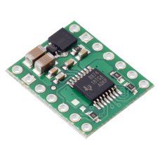
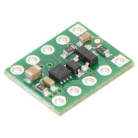
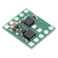
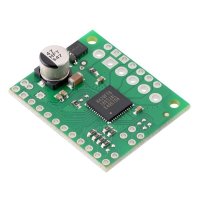
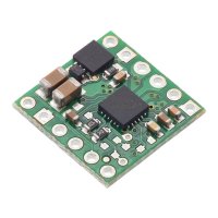
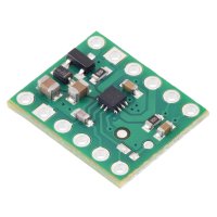
This compact breakout board for TI’s DRV8874/DRV8876/ DRV8876 (QFN)motor driver offers a wide operating voltage range of 4.5 V to 37 and can deliver a continuous 2.1 A (6 A peak)/1.3A (3.5 A peak)/1.1 A (3.5 Apeak) to a single bidirectional brushed DC motor. The DRV8874/DRV8876 /DRV8876 (QFN) also features integrated current sensing and regulation as well as built-in protection against under-voltage, over-current, and over-temperature. The carrier board adds protection against reverse voltage.
This product is a carrier board for Texas Instruments’ DRV887x family of motor drivers; we therefore recommend careful reading of the corresponding driver’s datasheet before using this product. Three pin-compatible versions are available that differ in the amount of current they can deliver while supporting the same 4.5 V to 37 V operating voltage ranges and control interfaces. The following table compares these three versions along with the similar DRV8256 motor drivers:
Details for item #4035/4036/4037:
This carrier for TI’s DRV8874PWP/DRV8876PWP/DRV8876RGT motor driver can supply continuous currents up to approximately 2.1 A/1.3 A/1.1 A and can tolerate peak currents up to 6 A/3.5 A/3.5 A. Since this board is a carrier for the DRV8874, we recommend careful reading of the DRV8874 datasheet/DRV8876 datasheet/DRV8876 datasheet. The board ships populated with all of its SMD components, including the DRV8874/DRV8876/DRV8876.

Features:
- Drives a single bidirectional brushed DC motor or two unidirectional brushed DC motors
- Motor supply voltage: 4.5 V to 37 V
- Output current:
- DRV8876 (QFN): 1.1 A continuous (3.5 A peak)
- DRV8876: 1.3 A continuous (3.5 A peak)
- DRV8874: 2.1 A continuous (6 A peak)
- Supports 1.8 V to 5 V logic voltage (5.5 V max)
- Integrated current sensing and adjustable active current regulation
- Two current regulation mode options: cycle-by-cycle or fixed off time
- Three input control modes:
- Phase/enable (PH/EH)
- PWM (IN/IN)
- Independent half-bridge control
- Under-voltage lockout and protection against over-current and over-temperature
- Carrier board adds reverse-voltage protection
- Compact size (0.6″×0.7″)
Using the motor driver:
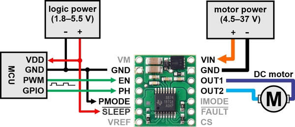
Motor and motor power connections are made on one side of the board and logic power and control connections are made on the other. The driver requires a motor voltage between 4.5 V and 37 V to be supplied to the VIN or VM pin. The driver is in sleep mode by default, and a logic voltage between 1.8 V and 5.5 V must be supplied to the SLEEP pin; to take it out of sleep mode. This logic voltage can typically shared with the controlling device, or it can be supplied by an output from the controlling device, which allows for dynamic control of the sleep mode. The VIN pin is the reverse-protected motor supply input and is the recommended point for connecting motor power. VM is an access point for motor supply power after the reverse voltage protection circuit.
The DRV8874/DRV8876 features three possible control modes: phase/enable (PH/EN), PWM (IN/IN), and independent half-bridge. The PMODE pin determines the control interface, and the state is latched when the driver is enabled through the SLEEP pin.
Phase/enable (PH/EN) mode:
Setting the PMODE pin low prior to enabling the driver, as shown in the diagram above, sets the driver to phase/enable control mode, where the PH pin determines the motor direction and the EN pin can be supplied with a PWM signal to control the motor speed (this is typically referred to as sign-magnitude operation). This mode is generally easier to use as it only requires one PWM signal, but it only allows for drive/brake operation. (Drive/brake operation usually provides a more linear relationship between PWM duty cycle and motor speed than drive/coast operation, and we generally recommend using drive/brake operation when possible.)
Simplified drive/brake operation with PMODE=0 (PHASE/ENABLE)
| EN | PH | OUT1 | OUT2 | Operating Mode |
| 0 | X | L | L | brake low (outputs shorted to ground) |
| PWM | 1 | PWM(H/L) | L | forward/brake at speed PWM % |
| PWM | 0 | L | PWM(H/L) | reverse/brake at speed PWM % |
This mode can also be used for locked-antiphase operation, where a sufficiently high-frequency (up to 100 kHz) PWM is applied to the phase (PH) pin and the enable (EN) pin is tied high. In locked-antiphase operation, the PWM duty cycle controls speed and direction, going from full-speed in one direction at 0% duty cycle to full speed in the other direction at 100% duty cycle. A duty cycle of 50% will stop the motor. The appropriate PWM frequency will generally depend on the inductance of the motor.
Advanced usage with PWM (IN/IN) mode: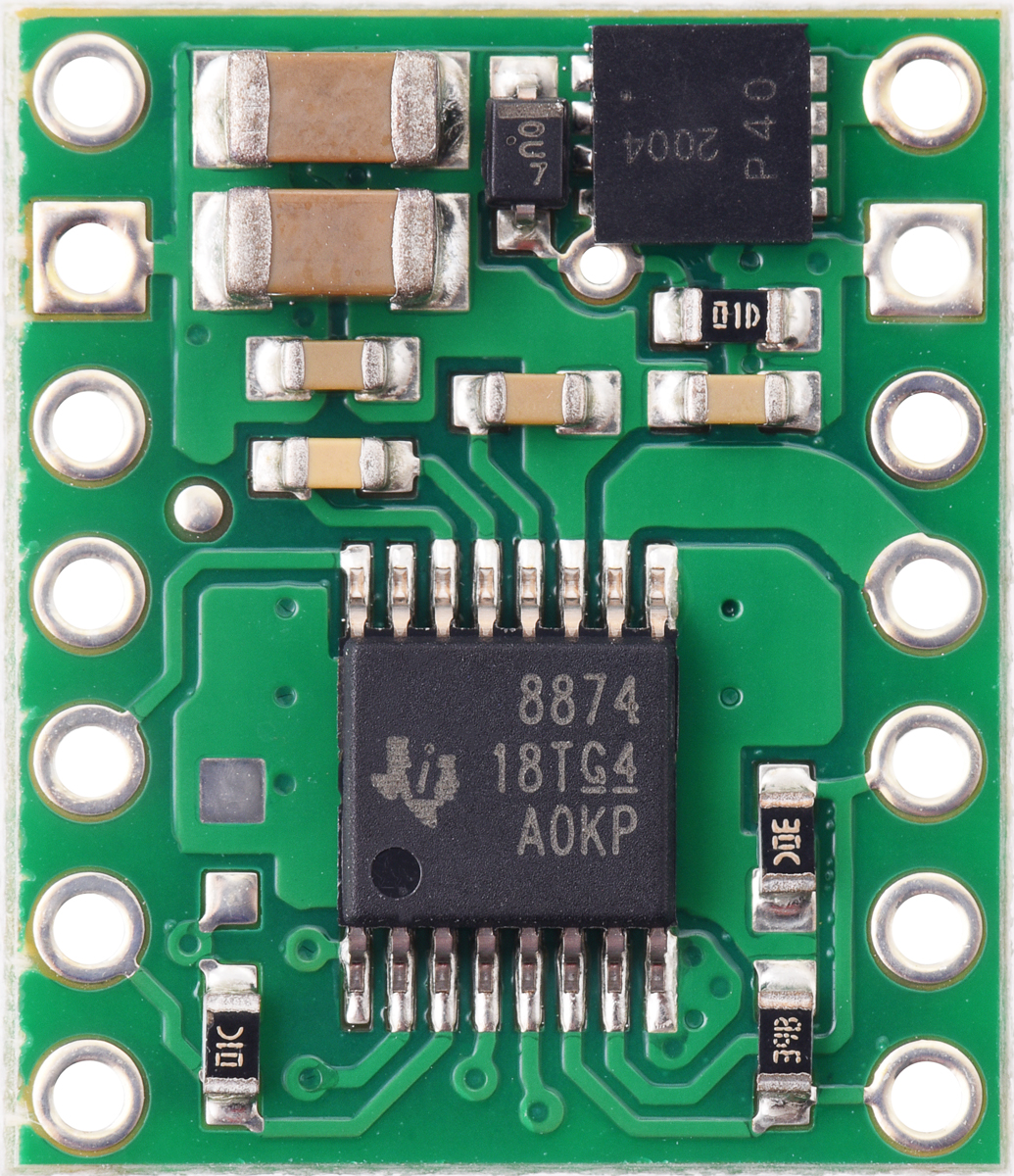
When the PMODE pin is set high prior to enabling the driver, the driver is set to PWM (IN/IN) control mode, which allows for more advanced control options, including allowing the H-bridge to enter a high-impedance (coast) state without having to put it to driver sleep. The following truth table show how to achieve drive/coast (slow decay) and drive/brake (fast decay) operation using the IN/IN control interface:
PWM control mode with PMODE=1 (IN/IN)
| IN1 | IN2 | OUT1 | OUT2 | Operating Mode |
| 0 | 0 | Z | Z | coast (outputs off) |
| PWM | 0 | PWM(H/Z) | PWM(L/Z) | forward/coast at speed PWM % |
| 0 | PWM | PWM(L/Z) | PWM(H/Z) | reverse/coast at speed PWM % |
| PWM | 1 | L | PWM(L/H) | reverse/brake at speed 100% − PWM % |
| 1 | PWM | PWM(L/H) | L | forward/brake at speed 100% − PWM % |
| 1 | 1 | L | L | brake low (outputs shorted to ground) |
Advanced usage with independent half-bridge mode:
When the PMODE pin is left high-impedance (i.e. floating or disconnected) when the driver is enabled, the driver is set to independent half-bridge control mode. See the DRV8874/DRV8876 datasheet for more information about this control mode.
PIN:
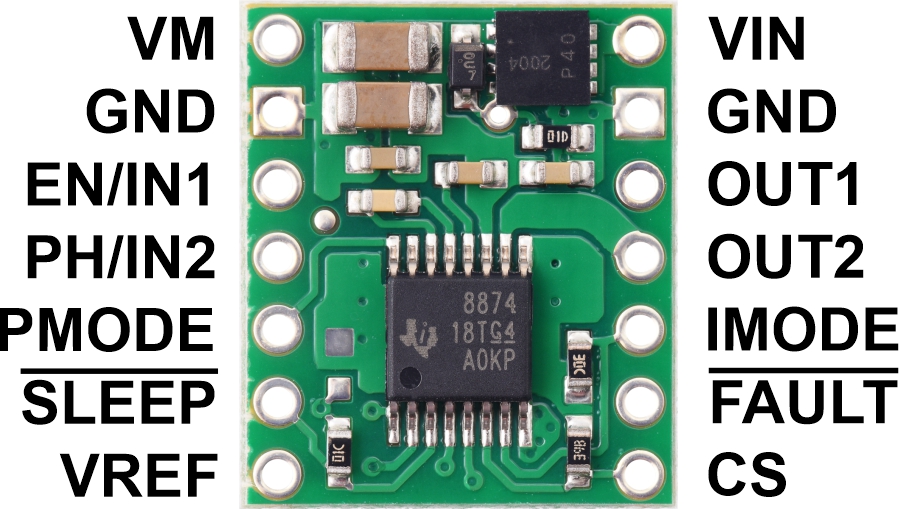
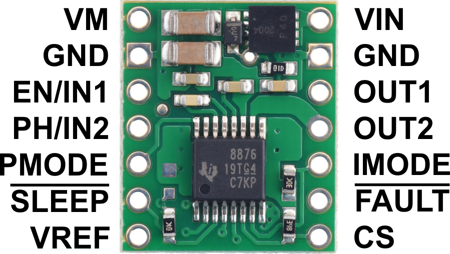
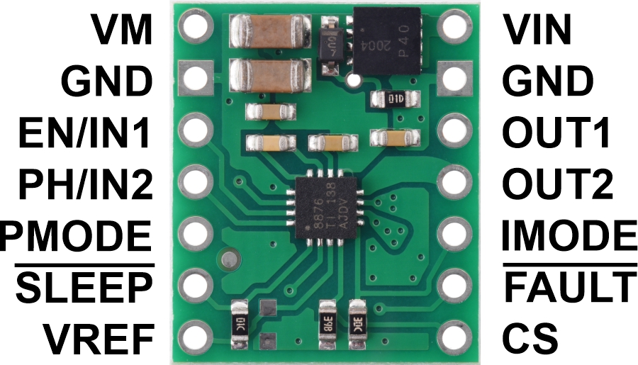
- VIN: 4.5 V to 37 V board power supply input.
- GND: Ground connection points for the motor and logic supplies. The control source and the motor driver must share a common ground.
- VM: This pin gives access to the motor power supply after the reverse-voltage protection MOSFET (see the board schematic below). It can be used to supply reverse- protected power to other components in the system.
- OUT1: Motor output 1.
- OUT2: Motor output 2.
- EN/IN1: LOW: Motor control input 1 (functions as an enable pin in PHASE/ENABLE mode).
- PH/IN2: LOW: Motor control input 2 (functions as a direction pin in PHASE/ENABLE mode).
- PMODE FLOATING: Control interface select pin. The state of this pin is latched when the driver is enabled through the SLEEP pin. Setting this pin low prior to enabling sets the driver to phase/enable (PH/EN) control mode. Setting this pin high prior to enabling sets the driver to PWM (IN/IN) control mode. Leaving this pin floating or disconnected on enable sets the driver to independent half-bridge control mode.
- SLEEP LOW: Sleep input that puts the driver into a low-power sleep mode when low. The driver outputs are high-impedance (coast) in sleep mode.
- VREF: Current limiting threshold reference voltage (see below).
- IMODE PULLED LOW: Four-state input for current regulation and overcurrent protection mode (see below). This carrier pulls down IMODE to GND through a 20 kΩ resistor setting the current chopping mode to cycle-by-cycle, the over-current response to automatic retry, and FAULT response to current chopping and over-current.
- FAULT FLOATING: Open-drain, active-low fault output. This pin goes low during an over-current, over-temperature, or under-voltage condition. An external pull-up resistor is required to use this pin.
- CS: Current sense output. This pin provides an analog current-sense feedback voltage of approximately 1.1 V/A (DRV8874) or 2.5 V/A (DRV8876).
- The actual current you can deliver will depend on how well you can keep the motor driver cool. The carrier’s printed circuit board is designed to help with this by drawing heat out of the motor driver chip. PWMing the motor will introduce additional heating proportional to the frequency.
Note:
- This product can get hot enough to burn you long before the chip overheats. Take care when handling this product and other components connected to it.
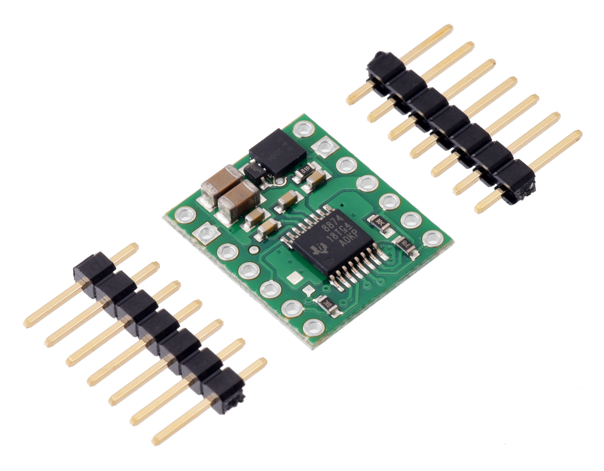
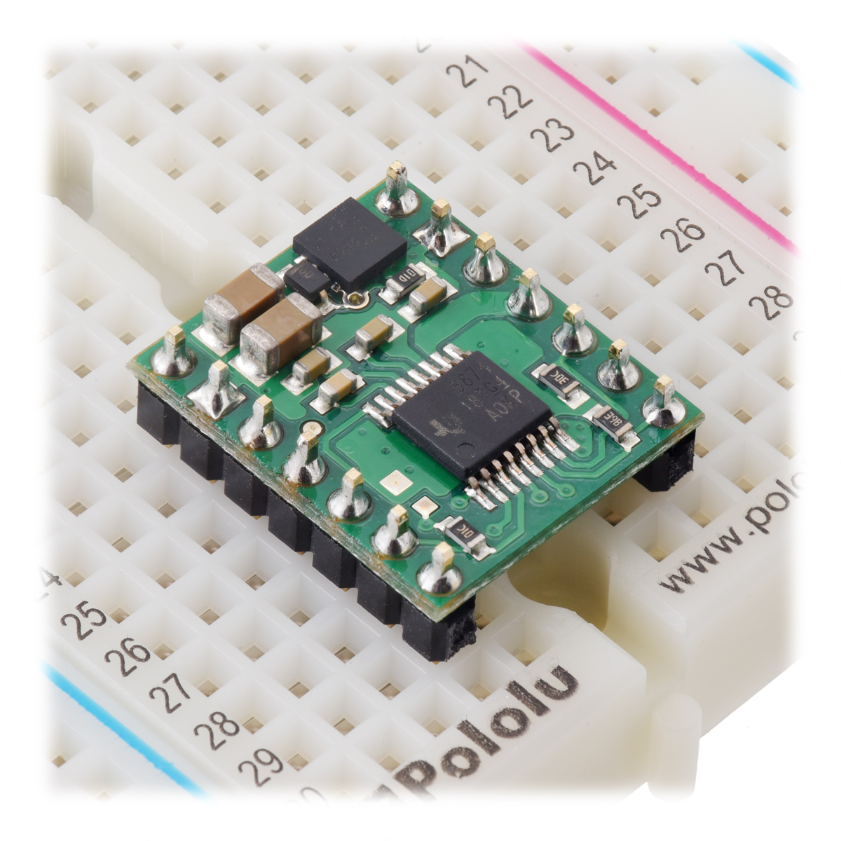
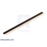
Breakaway 0.1″ male headers are included with the DRV8874/DRV8876 motor driver carriers, which can be soldered in to use the driver with perfboards, breadboards, or 0.1″ female connectors. (The headers might ship as a single larger strip that can be broken into smaller pieces.) When used with these header pins, the board can be oriented with the parts visible, as shown in the right picture above, or with the silkscreen visible, by soldering the headers in from the opposite side. You can also solder your motor leads and other connections directly to the board.
Schematic:
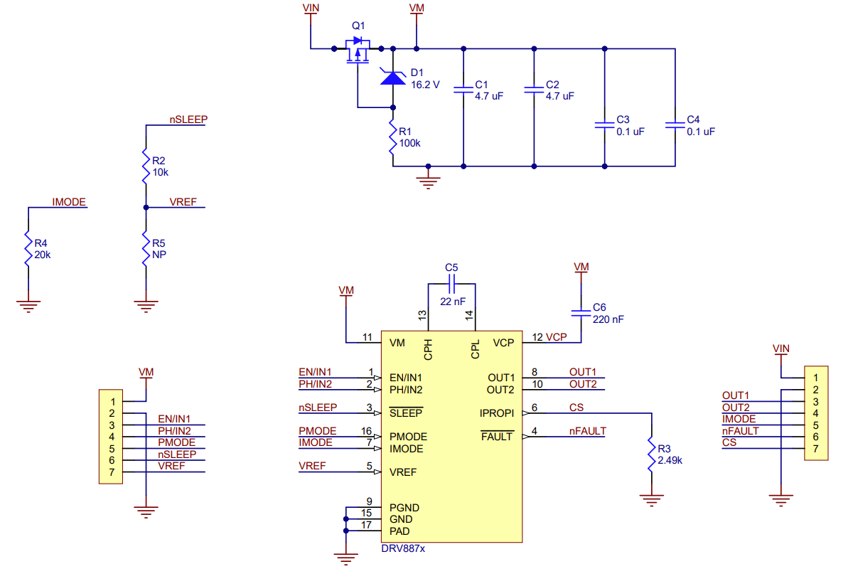
This diagram is also available as a downloadable pdf: DRV887x Single Brushed DC Motor Driver Carrier schematic (110k pdf).
Specifications:
- Specifications for DRV8874:
- Motor driver: DRV8874
- Motor channels: 1
- Minimum operating voltage: 4.5 V
- Maximum operating voltage: 37 V
- Continuous output current per channel: 2.1 A
- Peak output current per channel: 6 A
- Current sense: 1.13 V/A
- Maximum PWM frequency: 100 kHz
- Minimum logic voltage: 1.8 V
- Maximum logic voltage: 5.5 V
- Reverse voltage protection?: Y
- Header pins soldered?: N
- PCB dev codes: md41a
- Other PCB markings: 0J13404
- Size: 0.6″ × 0.7″
- Weight: 0.9 g1
- Specifications For DRV8876:
- Motor driver: DRV8876
- Motor channels: 1
- Minimum operating voltage: 4.5 V
- Maximum operating voltage: 37 V
- Continuous output current per channel: 1.3 A
- Peak output current per channel: 3.5 A
- Current sense: 2.49 V/A
- Maximum PWM frequency: 100 kHz
- Minimum logic voltage: 1.8 V
- Maximum logic voltage: 5.5 V
- Reverse voltage protection?: Y
- Header pins soldered?: N
- PCB dev codes: md41a
- Other PCB markings: 0J13404
- Size: 0.6″ × 0.7″
- Weight: 0.9 g1
- Specifications for DRV8876 (QFN):
- Motor driver: DRV8876
- Motor channels: 1
- Minimum operating voltage: 4.5 V
- Maximum operating voltage: 37 V
- Continuous output current per channel: 1.1 A
- Peak output current per channel: 3.5 A
- Current sense: 2.49 V/A
- Maximum PWM frequency: 100 kHz
- Minimum logic voltage: 1.8 V
- Maximum logic voltage: 5.5 V
- Reverse voltage protection?: Y
- Header pins soldered?: N
- PCB dev codes: md41b
- Other PCB markings: 0J13402
- Size: 0.6″ × 0.7″
- Weight: 0.8 g1
Documentation:
NOTE:
- Without included hardware.
Package Includes:
- 1 x Pololu 4035/4036/4037 Single Brushed DC Motor Driver Carrier DRV8874/DRV8876/DRV8876 (QFN)
Pololu 4035/4036/4037 Single Brushed DC Motor Driver Carrier DRV8874/DRV8876/DRV8876 (QFN)
- Brand: Pololu
- Product Code: Pololu-Single-DC-Motor-Driver
- Reward Points: 5
- Availability: In Stock
- रo 565.00
-
रo 542.00
- Price in reward points: 565
-
- 25 or more रo 539.00
- 96 or more रo 515.00
- 250 or more रo 496.00
Available Options
Related Products
Pololu 2990 DRV8838 Single Brushed DC Motor Driver Carrier
This tiny breakout board for TI’s DRV8838 motor driver can deliver a continuous 1.7 A (1.8 A peak) t..
रo 340.00 रo 354.00
Pololu 2961 MAX14870 Single Brushed DC Motor Driver Carrier
This compact breakout board for Maxim’s MAX14870 motor driver offers a wide operating voltage range ..
रo 754.00 रo 786.00
Solderless Breadboard Prototype 1660 Tie Points
Solderless Breadboard Prototype 1660 Tie Points Features: ..
रo 1,300.00
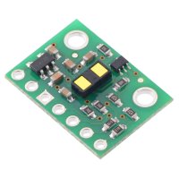
Pololu 2489/2490/3415/3416 Time-of-Flight Distance Sensor Carrier with Voltage Regulator VL53L0X/ VL53L1X/ VL6180X
These sensors are a carrier/breakout board for ST’s VL6180X, VL53L0X or VL53L1X laser-ranging sensor..
रo 1,022.00 रo 1,064.00
Pololu 2999 TB67H420FTG Dual/Single Motor Driver Carrier
The TB67H420FTG from Toshiba is an H-bridge motor driver IC that can be used for bidirectional contr..
रo 793.00 रo 944.00
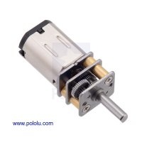
Pololu 4798 / 4799 380:1 Micro Metal Gearmotor HPCB 12V
This gearmotor is a miniature high-power, 12 V brushed DC motor with long-life carbon brushes and a ..
रo 1,702.00 रo 1,773.00
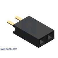
Pololu 1012/1013/1014/1015/1016/1017/1018/1019/1020/1021/1030/1031/1111 0.100 inch (2.54 mm) Female Header
These 0.1" straight female header strips are commonly used as low-cost connectors for custom-made ca..
रo 34.00
Pololu 965 / 2664 / 2665 / 2666 / 2667 0.100 inch (2.54 mm) Breakaway Male Header: 1×40-Pin, Straight
These 0.1″/2.54mm-pitch header strips are commonly used as low-cost connectors. The standard spacing..
रo 72.00 रo 75.00
Pololu 4038 DRV8256E Single Brushed DC Motor Driver Carrier
Texas Instruments’ DRV8256E is a tiny H-bridge motor driver IC that can be used for bidirectional co..
रo 1,085.00 रo 1,130.00
Pololu 4733 MP6550 Single Brushed DC Motor Driver Carrier
This tiny breakout board for the MPS MP6550 motor driver offers a wide operating voltage range of 1...
रo 376.00 रo 391.00
Tags: Pololu, Single Brushed, Brushed, DC Motor, Driver Carrier

